JFET输入低噪声放大电路
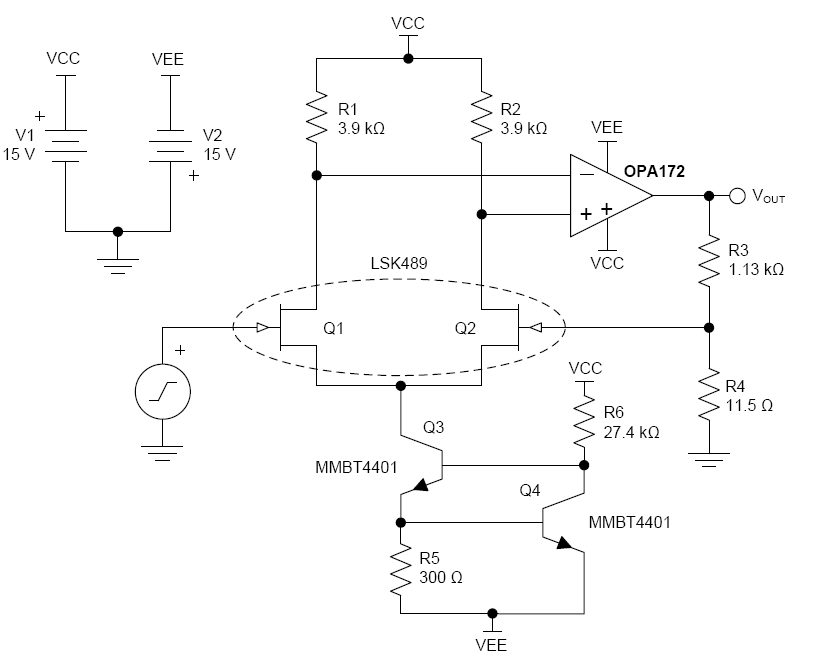
this diagram shows a low-noise composite amplifier built by adding a
low noise JFET pair (Q1 and Q2) as an input
preamplifier for the OPA172. Transistors Q3 and Q4 form a 2-mA current sink
that biases each JFET with 1 mA
of drain current. Using 3.9-kΩ drain resistors produces a
gain of approximately 10 in the input amplifier, making
the extremely-low, broadband-noise spectral density of the JFET pair, Q1 and
Q2, the dominant noise source of
the amplifier. The output impedance of the input differential amplifier is large
enough that a FET-input amplifier
such as the OPA172 provides superior noise performance over bipolar-input amplifiers.
复合放大器的增益由如下公式计算出来:
AV = (1 + R3 / R4)
The resistances shown are standard 1% resistor values that produce a gain of
approximately 100 (99.26) with
68° of phase margin. Gains less than 10 may require additional compensation
methods to provide stability.
Select low resistor values to minimize the resistor thermal noise contribution
to the total output noise.
应用:
电源模块内的跟踪放大器 Tracking Amplifier in Power Modules
商用电源 Merchant Power Supplies
传感器放大器 Transducer Amplifiers
桥式放大器 Bridge Amplifiers
温度测量 Temperature Measurements
应力计放大器 Strain Gauge Amplifiers
精密积分器 Precision Integrators
测试设备 Test Equipment
TI的OPA172规格书带参考设计下载(第26页)
LSK489技术&商务&样品&评估板咨询 => 座机 0755-82565851 邮件dwin100@dwintech.com 手机156-2521-4151
![]() D-Win Technology(HongKong) Co.,Ltd 深圳市南频科技有限公司 回首页
D-Win Technology(HongKong) Co.,Ltd 深圳市南频科技有限公司 回首页